exercise 4.1
ZIP with MATLAB scripts and note:

Question:
exercise 4.1 notes:


Answer:
Contents
1.- Simplified approach
2.- Example Modal Analysis and Mode Matching Method
3.- Models built with Modal Analysis and mode matching
Symmetric horizontal fin
Asymmetric horizontal fin
Symmetric horizontal thick hurdle
Asymmetric horizontal thick hurdle
Symmetric and Asymmetric horizontal b step [DBR]
Asymmetric horizontal b step [COLL1]
Asymmetric horizontal b step [RAMO]
4.- Waveguide b step modelled with fin interface
5.- Waveguide b step modelled with thick hurdle
6.- Wave Insertion in Rectangular Waveguides
7.- 2D FEM Solution [OZKU]
Shorted Load
Matched Load
Tilted Feed
Below cut-off
8.- Limitation of Eigen-modes in 2D Conformal Mapped Domain
9.- REMCOM Mode Converters
10.- Wave Incidence Angles on sidewalls inside Waveguides
Comment: I was about to include in this solution another point with [ED] FDTD, but I am using FDTD to solve other [POZAR] exercises, and time spent on this exercise went through the roof, [POZAR] has 338 exercises and 104 examples. So FDTD for this exercise left for next version of this solution.
1.- Simplified approach
According to [POZAR] the apparently time saving approach to solve this exercise is to ignore that the system is a 3D wave propagating in a 3D waveguide with 3D obstacles, abstracting to transmission line (TEM), and apply [POZAR] table (3.2) shown on right hand side.

Let's select for instance, from [HM1] the following air cooled waveguide: WR137 part number 14-LA-9020.
With operating band f=[5850 8200] % MHz WG14 [2][KC1][ERF24][NMAU][3]. Note that off-the-shelf [HM1] waveguide comes in z sections with regular length: 375mm. So if you design with multiples of such section length, some cutting/flanging may be saved, as well as no need making sure that deformations have been caused by custom made waveguide length. It's always worth ask waveguide suppliers to carry out such customised lengths.

The flaw in such over-simplification is that after going through [POZAR] (table 3.2), as follows
eps0 =8.854187817e-12; % [F/m]=[C^2/N*m^2] permittivity empty space and dry air
mu0 =4*pi*1e-7; % [H/m]=[T*m/A] permeability in empty space and dry air
er=1;
mur=1;
c0=1/(eps0*mu0)^.5 % [m/s] light speed
etha0=(mu0*mur/(eps0*er))^.5
% example 4.2
% initial check that with example 4.2 then Z0=500
% a=22.86e-3
% b=10.16e-3
% f0=1e10 % [Hz] example 4.2
% er=2.54
a=35e-3 % 35mm, horizontal, rectangular waveguide WR137
b=16e-3 % 16mm, vertical, rectangular waveguide WR137
f0=6e9 % [Hz] carrier
lambda0=c0/f0
sigma_cu = 5.813e7 % assume Copper
d_skin=1/(pi*f0*mu0*sigma_cu).^.5 % skin depth
m=1;n=0; % TEmn m=1 n=0
k0=2*pi*f0*(mu0*eps0*mur*er)^.5 % rectangular waveguide
k0_TE=k0_TM
k0=2*pi/lambda0
kc=((m*pi/a)^2+(n*pi/b)^2).^.5
fc=c0/(2*pi*er^.5)*((m*pi/a)^2+(n*pi/b)^2).^.5
beta=(er*k0.^2-kc^2).^.5
labmdac=2*pi./kc % cut-off wavelength
lambdag=2*pi./beta % group propagation wavelength
vp=2*pi*f0./beta % wave propagation velocity
alphad=k0^2*tand(d_skin)./(2*beta) % attenuation caused by metal
Z0=k0*etha0/beta
%%
b2=b/2
kc2=((m*pi/a)^2+(n*pi/b2)^2).^.5
fc2=c0/(2*pi*er^.5)*((m*pi/a)^2+(n*pi/b2)^2).^.5
beta2=(k0.^2-kc2^2).^.5
labmdac2=2*pi./kc2 % cut-off wavelength
lambdag2=2*pi./beta2 % group propagation wavelength
vp2=2*pi*f0./beta2 % wave propagation velocity
alphad2=k0^2*tand(d_skin)./(2*beta2) % attenuation caused by metal
etha02=etha0 % since not mentioned 2nd waveguide b/2
Z02=k0*etha02/beta2
c0 = 2.997924580105029e+08
etha0 = 3.767303134749689e+02
a = 0.035000000000000
b = 0.016000000000000
f0 = 6.000000000000000e+09
lambda0 = 0.049965409668417
sigma_cu = 58130000
d_skin = 8.522055239991091e-07
k0 = 1.257507013126954e+02
k0 = 1.257507013126954e+02
kc = 89.759790102565503
fc = 4.282749400150041e+09
beta = 88.070534013244810
labmdac = 0.070000000000000
lambdag = 0.071342650269779
vp = 4.280559016186730e+08
alphad = 1.335309438599717e-06
Z0 = 5.379109103403914e+02
b2 = 0.008000000000000
kc2 = 89.759790102565503
fc2 = 4.282749400150041e+09
beta2 = 88.070534013244810
labmdac2 = 0.070000000000000
lambdag2 = 0.071342650269779
vp2 = 4.280559016186730e+08
alphad2 = 1.335309438599717e-06
etha02 = 3.767303134749689e+02
Z02 = 5.379109103403914e+02
one realises that despite waveguide changing b to b/2 then beta (left) and beta2 (right) seem to have same values on both sides of b step.
Apparently, TE and TM have same characteristic impedances Z0 and Z02.
It is obvious that b/2 metal wall opposing incident traveling wave bounces back certain power percentage of any incident wave.
Yet Z01==Z02 means reflection coefficient caused by b step interface or transition would be null, that it is not.
For a wave travelling left to right inside rectangular waveguide, the obstacle of finding half waveguide section suddenly stepped down from b to b/2 generates bouncing fields that are no longer transversal.
For this exercise [POZAR] solutions manual briefly suggests 'higher modes to be considered' and then hops to next exercise.
In rectangular waveguides, TE TM modes with same [m n] indices have same TE TM cut-off frequencies values. But such is not the case for characteristic impedances: Z0_TE and Z0_TM that are different even for TE TM modes with identical [m n] indices.
M=3; % top M mode to check
N=3; % top N mode to check
Nrange=[0:1:N];
Mrange=[0:1:M];
nL=combinator(numel(Mrange),2,'p','r') % permutations with repetition
MNrange=[Mrange([nL(:,1)'])' Nrange(nL(:,2))'] % no need for double for loops
kc=((MNrange(:,1)*pi/a).^2+(MNrange(:,2)*pi/b).^2).^.5
fc=c0/(2*pi*er^.5)*((MNrange(:,1)*pi/a).^2+ (MNrange(:,2)*pi/b).^2).^.5 % cut-off frequencies
beta=imag((er*k0.^2-kc.^2).^.5) % propagation constants when alpha=0
labmdac=2*pi./kc % cut-off wavelengths
lambdag=2*pi./beta % group propagation wavelengths
vp=2*pi*f0./beta % wave propagation velocities
alphad=real(k0^2*tand(d_skin)./(2*beta)) % attenuation caused by metal
Z0_TE=k0*etha0./beta % characteristic impedance of TE TH propagating modes
Z0_TM=beta*etha0/k0
fc_=[fc;fc]; % putting together all TE TH parameters
m_=[MNrange(:,1);MNrange(:,1)]
n_=[MNrange(:,2);MNrange(:,2)]
L1=num2str([ones(1,numel(Nrange([nL(:,1)])))'; zeros(1,numel(Nrange([nL(:,1)])))']);
L1=strrep(L1','1','E');
L1=strrep(L1,'0','H')';
beta_=[beta;beta];
vp_=[vp;vp];
lambdag_=[lambdag;lambdag];
Z0_=[Z0_TE;Z0_TM];
Such chosen WR137 rectangular waveguide has upper recommended band limit 8.2GHz a bit below TE20 and TH20 cut-off frequencies 8.5GHz.
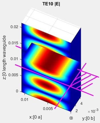
So at f0 6GHz there are no upper modes, yet the 'wall' halving waveguide dimension b is going to bounce back a significant amount of wave energy, at a certain distance of the sharp b step there may or may not be 'higher modes', yet there is energy storage nearby b step discontinuity. Such energy storage caused by discontinuities like pipe bents, or in microstrip devices like a DRO close enough to act as resonating cavity, are often in literature referred as 'evanescent' fields. Telling whether containing higher modes or not is a basic exercise of counting E peaks and H loops across a given waveguide cross section as detailed in [RAMO] pg414. Evanescent fields have to do with g=a+jb purely real, g propagation constant a attenuation due to metal and dielectric, and b propagation constant: an evanescent field is a field in cut-off, not propagating, just attenuating [WRNK].
From fc=c0/(2*pi*er^.5)*((m*pi/a)^2+(n*pi/b)^2).^.5 halving b with sharp step does not affect lowest cut-off fc for TE10.
So it's not just that 'higher modes' are responsible for reflection coefficient on b sharp transition and turn page to next exercise, which 'higher modes' would be? It's the z travelling wave bouncing back on b step face behaving as mirror, along with sharp metal surface angles either forcing fields fold onto similar direction they come from (concave corner), or scatter on all possible directions (convex corner), diverting wave energy away from main travelling direction. Since waveguides are used to transport signals, left to right, from generator to load, TE10 abs(E) in rectangular waveguides shows static peaks along z measurable maxima and minima (introduce probe through slot on minima to minimise fields perturbation). If this waveguide is used as part of a resonant cavity, then the z point where such b step is implemented will cause maximal disturbance if affecting a field peak that will be bounced back and scattered, but a lower amplitude.
Also, if b step is implemented right on z=n*lambda/2 where TE10 E field is theoretically null there shouldn't be much wave bounced back, neither concave nor convex 90º would cause much reflection .
Next, for a waveguide z length 37.5mm long L=0.375 and lambda0=c0/f0 then
Solution to [POZAR] example 3.1.3 TE10 [POZAR] pg118


Heading 6
If we have control over f0 carrier value, one could bring abs(E) minima to take place where b step is located:
on the halved waveguide section
If one tries to squeeze in another lambda/2 or lambda
L=.375 % waveguide section length
c0/f0;lambda0
L/lambda0
lambda02=L/7.5
f02=c0/lambda02
lambda03=L/8
f03=c0/lambda03
lambda04=L/8.5
f04=c0/lambda04
lambda0 = 0.049965409668417
=7.505192141695486
lambda02 = 0.050000000000000
f02 = 5.995849160210057e+09
lambda03 = 0.046875000000000
f03 = 6.395572437557395e+09
lambda04 = 0.044117647058824
f04 = 6.795295714904732e+09
Band edges
f1=5850e6; % [Hz]
f2=8200e6; % [Hz]
% lower limit to implement b/2 step
lambda_f1=c0/f1
L/lambda_f1
lambda_f1_1=L/7
f1_1=c0/lambda_f1
% upper limit to implement b/2 step
lambda_f2=c0/f2
L/lambda_f2
lambda_f2_1=L/10
f2_1=c0/lambda_f2_1
Choosing 11.0 GHz carrier, or even 10.5 GHz both be out of band then:
lambda_f2_1=L/10.5
c0/lambda_f2_1
lambda_f2_1=L/11
c0/lambda_f2_1
lambda_f1 = 0.051246574018889
= 7.317562338153099
lambda_f1_1 = 0.053571428571429
f1_1 = 5.850000000000000e+09
lambda_f2 = 0.036560055854939
= 10.257095926983830
lambda_f2_1 = 0.037500000000000
f2_1 = 7.994465546946744e+09
Another function that may result useful to find out where to cut is numden . Here [n1,d1]=numden(sum(L)) % n1/d1=L means n1=3;d1=8
Solution to [POZAR] example 3.1.3 TE11 different cross-section but same as [DBR] pg59 TE11
[DBR] pg59 rectangular waveguide cross sections are a bit more accurate compared to [POZAR] pg118 in regard of one being able to qualitatively tell around what z points along propagation axis fields are strong or weak.

Both 90º (convex) and 270º (concave) corners, perpendicularly obstructing E field, do store energy. This is opposite to changing horizontal dimension with a step, where obstacles are parallel to E field increasing current thus showing inductive behaviour, not storing but increasing consumption.
TE TM cut-off frequencies ordered with increasing frequency.
T=table(fc_,m_,n_,L1,beta_,vp_,lambdag_,Z0_);
T=sortrows(T,1)
T =
32×9 table
fc M N Tmode beta vp lambdag Z0 alpha
________________ _ _ ____ ________________ ________________ ___________________ _____________ ____________
0 0 0 E 0 Inf Inf Inf Inf
0 0 0 H 0 Inf Inf 0 Inf
4282749400.15004 1 0 E 0 Inf Inf Inf Inf
4282749400.15004 1 0 H 0 Inf Inf 0 Inf
8565498800.30008 2 0 E 128.117293119983 294254670.271342 0.0490424450452236 369.771324163573 9.17919919056267e-07
8565498800.30008 2 0 H 128.117293119983 294254670.271342 0.0490424450452236 383.82026895132 9.17919919056267e-07
9368514312.82821 0 1 E 150.797557377832 249998159.775361 0.0416663599625602 314.156952864497 7.79862866317828e-07
9368514312.82821 0 1 H 150.797557377832 249998159.775361 0.0416663599625602 451.766952145618 7.79862866317828e-07
10301019505.5709 1 1 E 175.489951935651 214822053.497975 0.0358036755829958 269.953354039325 6.701319023298e-07
10301019505.5709 1 1 H 175.489951935651 214822053.497975 0.0358036755829958 525.74167709831 6.701319023298e-07
12693968257.7045 2 1 E 234.450811446979 160797531.944576 0.0267995886574294 202.064138028981 5.01603788891124e-07
12693968257.7045 2 1 H 234.450811446979 160797531.944576 0.0267995886574294 702.379603205953 5.01603788891124e-07
12848248200.4501 3 0 E 238.113713155448 158323984.551307 0.0263873307585512 198.95578670138 4.93887621052844e-07
12848248200.4501 3 0 H 238.113713155448 158323984.551307 0.0263873307585512 713.353109472355 4.93887621052844e-07
15901149085.8377 3 1 E 308.628065127639 122150627.57655 0.020358437929425 153.499005690349 3.81045759016656e-07
15901149085.8377 3 1 H 308.628065127639 122150627.57655 0.020358437929425 924.603572854749 3.81045759016656e-07
18737028625.6564 0 2 E 372.020604115399 101336085.759872 0.0168893476266454 127.342681026704 3.16115328101354e-07
18737028625.6564 0 2 H 372.020604115399 101336085.759872 0.0168893476266454 1114.51814856314 3.16115328101354e-07
19220254528.5736 1 2 E 382.695897293978 98509317.9980394 0.0164182196663399 123.790459893113 3.07297298356101e-07
19220254528.5736 1 2 H 382.695897293978 98509317.9980394 0.0164182196663399 1146.49973199465 3.07297298356101e-07
20602039011.1419 2 2 E 413.069739346049 91265731.3091025 0.0152109552181837 114.687900402071 2.84701114917263e-07
20602039011.1419 2 2 H 413.069739346049 91265731.3091025 0.0152109552181837 1237.49522480914 2.84701114917263e-07
22719016781.9613 3 2 E 459.250159673022 82088402.2553604 0.0136814003758934 103.155328588146 2.56072671622223e-07
22719016781.9613 3 2 H 459.250159673022 82088402.2553604 0.0136814003758934 1375.8448645692 2.56072671622223e-07
28105542938.4846 0 3 E 575.469409130636 65510192.6269717 0.0109183654378286 82.3225359568586 2.04357370634287e-07
28105542938.4846 0 3 H 575.469409130636 65510192.6269717 0.0109183654378286 1724.02037232338 2.04357370634287e-07
28429975137.0185 1 3 E 582.427558383375 64727555.0417252 0.0107879258402875 81.3390445615652 2.01915952701183e-07
28429975137.0185 1 3 H 582.427558383375 64727555.0417252 0.0107879258402875 1744.86594790925 2.01915952701183e-07
29381785404.6507 2 3 E 602.820305333347 62537893.1491545 0.0104229821915257 78.5874342753469 1.95085358422643e-07
29381785404.6507 2 3 H 602.820305333347 62537893.1491545 0.0104229821915257 1805.95957101339 1.95085358422643e-07
30903058516.7128 3 3 E 635.355349484422 59335475.6100969 0.00988924593501615 74.5631577095747 1.85095498803676e-07
30903058516.7128 3 3 H 635.355349484422 59335475.6100969 0.00988924593501615 1903.42970242425 1.85095498803676e-07
2.- Example Modal Analysis and Mode Matching Method
Inductive a step
[POZAR] pages 204 to 209 contain rectangular wave a step, also referred as rectangular waveguide H-plane step, or inductive step.
[POZAR] assumes that TE10 exciting waveguide from left side is only propagating to the 2nd section a2=a1/2 in TEn0 modes, yet:
-
Despite calling the exciting signal 'TE', the magnetic component of the input field is only conceived as Hx component, thus input wave is TEM.
-
Flange metal corners have both vertical and horizontal lines. Such corners, either convex or concave are waveguides 'per se', implying that despite a vertical E field hitting such local 'waveguides', some wave energy is funnelled horizontally from the impact point on, along whatever horizontal length is allowed to run onto.
In radar such sharp surface angles and corner become distinctive part of cross-sections uniquely identifying targets, thus such discontinuities do reflect propagating signal too and the signal level of such sharp corners
and edges may be higher than signal reflected returning off flat surfaces.
-
Same applies to Ex horizontally hitting a vertical corner, why is it assumed propagating Ey in zone 1 does only generate propagating Ey in zone 2? don't know the answer but I consider it again an oversimplification that works only if the waveguide feed is straight-up enough and aligned enough to pump in the waveguide Ey and Hx only.
-
Literature sources refer to 'local' evanescent fields, or 'degenerated modes' when the propagation constant goes from complex to real, then such fields do not propagate, but such incident energy may still run along sharp angles (convex or concave) as long as the cut-off attenuation constant that the propagation constant is turned into, allows them to do so. In fact there are successful vehicles on the road that on purpose use optical network in cut-off, in field attenuation modes, by design, to make available just the intended amount of energy to receiving modules, without incurring propagation that in case of damaged line ('pealed, bent, broken, ..) would cause undesired signal radiation. Because if a propagating signal reaches a breached waveguide point, almost inevitably, that point becomes an antenna. Antenna developers call such technology 'leaky' antennas; when carefully pierced/slotted waveguides are turned into antennas.
-
The question of this exercise does not mention any relative permittivity or permeability, therefore assuming void waveguide or dry air.
[POZAR] pg208 claims graph agreement with [DBR] pg168 (1st case [DBR] chapter 4) graph trace lambda0/a=1.4 despite [POZAR] does not show at all any frequency or lambda0 throughout the only modal analysis explanation in the entire book.
[DBR] supplies 2 graphs for rectangular waveguide a step, pg169 and pg171.
Despite [DBR] arguing that pg169 measurements are old, and that readers attention should focus on pg171 analytical results, the following MATLAB lines reach X*lambda0/(Z0*2*a)=1.18 agree with [DBR] pg169 lambda0/a=1.4 trace.
On far right hand side [POZAR] quoting [DBR] modal graph.
[DBR] pg169 [DBR] pg171
Nmax=5 % highest TEn0
n=[1:Nmax]
a1=35e-3 % left side
a2=a1/2
b=16e-3
c0=3e8 % [m/s] light speed
etha0=120*pi
f0=8e9 % [Hz]
lambda0=c0/f0 % wavelength
k0=2*pi/lambda0 % wave number

If a2=a1/2 then zone 1 incident wave doesn't make it to zone 2 in propagation, just cut-off
% beta(i,j) i:1 left zone, 2 right zone. j: TEj0 mode
beta=[(k0^2-(n*pi/a1).^2).^.5 ;
(k0^2-(n*pi/a2).^2).^.5]
% Z(i,j) i:1 left zone, 2 right zone. j: TEj0 mode
Z=k0*etha0./beta.^2
beta =
1.0e+02 *
Columns 1 through 3
0.8795 + 0.0000i 0.0000 + 1.2820i 0.0000 + 2.3816i
0.0000 + 1.2820i 0.0000 + 3.3633i 0.0000 + 5.2369i
Columns 4 through 5
0.0000 + 3.3633i 0.0000 + 4.3085i
0.0000 + 7.0700i 0.0000 + 8.8876i
Z =
6.1250 -2.8824 -0.8352 -0.4188 -0.2552
-2.8824 -0.4188 -0.1727 -0.0948 -0.0600
Widening 2nd waveguide cross-section to a2=a1*2/3 still doesn't allow anything but evanescent through to 2nd waveguide section.
a2=a1*2/3
beta=[(k0^2-(n*pi/a1).^2).^.5 ;
(k0^2-(n*pi/a2).^2).^.5]
Z=k0*etha0./beta.^2
beta =
1.0e+02 *
Columns 1 through 3
0.8795 + 0.0000i 0.0000 + 1.2820i 0.0000 + 2.3816i
0.0000 + 0.4834i 0.0000 + 2.3816i 0.0000 + 3.8387i
Columns 4 through 5
0.0000 + 3.3633i 0.0000 + 4.3085i
0.0000 + 5.2369i 0.0000 + 6.6137i
Z =
6.1250 -2.8824 -0.8352 -0.4188 -0.2552
-20.2759 -0.8352 -0.3215 -0.1727 -0.1083
and the 1st a1/a2 ratio that I catch allowing wave through both sections (strangling a) is
a2=a1*3/4
beta=[(k0^2-(n*pi/a1).^2).^.5 ; (k0^2-(n*pi/a2).^2).^.5]
Z=k0*etha0./beta.^2
beta =
1.0e+02 *
Columns 1 through 3
0.8795 + 0.0000i 0.0000 + 1.2820i 0.0000 + 2.3816i
0.3832 + 0.0000i 0.0000 + 2.0372i 0.0000 + 3.3633i
Columns 4 through 5
0.0000 + 3.3633i 0.0000 + 4.3085i
0.0000 + 4.6193i 0.0000 + 5.8506i
Z =
6.1250 -2.8824 -0.8352 -0.4188 -0.2552
32.2683 -1.1415 -0.4188 -0.2220 -0.1384
So what are the propagation/attenuation waveguide width a thresholds, for each considered mode
a1_ov_a2=[] % a1/a2
a1_ov_a2_nd=[0 0] % rat(a1/a2) in num/den form
syms a2_
for k1=1:1:numel(n)
eq1=(k0^2-(n(k1)*pi/a2_).^2)^.5==0
a1_ov_a2=double(solve(eq1,a2_))/a1;
[num1,den1]=numden(sym(a1_ov_a2(a1_ov_a2>0)))
a1_ov_a2_nd=[a1_ov_a2_nd;num1 den1];
end
a1_ov_a2_nd(1,:)=[];
a1_ov_a2
a1_ov_a2_nd'
a1_ov_a2 =
0.7143 1.4286 2.1429 2.8571 3.5714
=
[ 5, 10, 15, 20, 25]
[ 7, 7, 7, 7, 7]
While a narrower a (wider than a2/a1=5/7) it seems as the only way to get higher modes propagating onto second waveguide section, with inductive (a step) is widening a2/a1>1. Next higher mode may not show up propagating through 2nd waveguide section until a2/a1=10/7.
Now calculating General Scattering Matrix (GSM) coefficients A and B. GSM compiles propagation coefficients of multiple modes.
IN1 is support function for functions 'multiplication', a.k.a measure of degree of orthogonality: sin(n*pi*x/a)*sin(m*pi*x/a).
[POZAR] tags this integrals Ikn or Inm while [DBR] more accurately calls them V or I because such products are proportional to voltages and currents resulting sum of E loop integrals, and H area integrals respectively, details, right at beginning of [DBR] chapter 1 section 1.2.
function y=IN1(k1,ad1,k2,ad2)
ad=min(ad1,ad2)
fun1=@(x,k_1,k_2,ad1_,ad2_)
sin(k_1*pi*x/ad1_).*sin(k_2*pi*x/ad2_)
y=integral(@(x) fun1(x,k1,k2,ad1,ad2),0,ad)
end
dx=a1/50
x=[0:dx:a1];
y=[0:dx:b];
% support function IN1= integral(sin(k1*pi*x/ad1).*sin(k2*pi*x/ad2))
IN=zeros(Nmax)
for k1=n
for k2=n
IN(k1,k2)=IN1(n(k1),a1,n(k2),a2)
end
end
Q=zeros(Nmax)
for k3=n
for k4=n
Q(k3,k4)=2/(a2*Z(1,k4))*sum(IN(n,k3).*IN(n,k4).*Z(2,:)')
end
end
Q=Q+a1/2*eye(Nmax)
P=zeros(Nmax,1)
for k5=n
P(k5)=2/(a2*Z(1,1))*sum(IN(n,k5).*IN(n,1).*Z(2,:)')
end
A=inv(Q)*P
A contains reflected wave coefficients, for each mode, the a coefficient (not waveguide size) when defining scattering parameters s_ij=a_i/b_j
equivalent reactance
Xabs=Z(1,1)*(1+A(1))/(1-A(1)) Xabs = -54.324597993510594
pondered equivalent reactance, as graphed in [DBR] pg171 real measurements
Xabs*lambda0*1/(2*a1*Z(1,1)) = -6.335230086706776
pondered reactance result matches [DBR] transmission coefficients for all modes up to Nmax for f0=6e9
B=zeros(size(A));
for k2=1:1:numel(A)
B(k2)=-2*Z(2,k2)/a2*(-1/Z(1,1)* ...
IN1(k2,a1,1,a2)+sum(A(:)'./Z(1,:).* ...
IN1(k2*ones(1,numel(n)),a1,n,a2)));
end
A
B
A =
1.254151497314340
-0.198608799020959
0.113344379692468
-0.080717563620261
0.075996356182824
B =
1.515966166349444
0.213484610239494
-0.024333028994216
-0.030128796347184
0.027606324539843
Because in this exercise I also show [DBR] pg307 erroneous expression for rectangular waveguide b step needed for this exercise (Symmetric and Asymmetric b step), I actually consider [DBR] pg169 measurements for inductive a step to be more reliable than any analytical calculation in [DBR] chapter 4 1st case: old does not necessarily mean obsolete.
Checking on structure modes only without considering specific input signals is only one part of the problem about finding out whether a waveguide is going to let certain modes through, or certain polarisation only.
Cut-off frequencies have been checked with the fc formula for rectangular cavity, for constant cross-section. Yet B coefficients tell that despite a2/a3=2/3 that shouldn't let signal propagating
Capacitive b step
half way on paper.
3.- Models built with Modal Analysis and Mode Matching
Waveguides containing fins parallel to perpendicular waveguide cross-sections, in literature are often also referred as irises, thin hurdles, or diaphragms. Such obstacles are not sharp a or b size changes (size steps) but relatively thin obstacles, relative to waveguide size along propagating dimension z.
Such internal obstacles are useful to build waveguide splitters, combiners, and filters. Although not waveguide size step changes, just obstacles to propagating waves, some (thin) obstacles show similar local impedance behaviour, around a given discontinuity point, to for instance the sharp b step asked in this exercise.
More expensive but more reliable, if one has the relevant test instruments, devices and time to collect measurements, it would be to proceed the following way: 1.- build different prototypes 2.- measure real devices 3.- fit curves, and 4.- present formulas as the available models. But such approach alone is often, just for one particular application, ground for theses, building such DUT is time consuming and there are not so many network analysers around, even with the proliferation of software VNAs (Anritsu pocket VNA..).
[DBR] is a mix of analytical and numerical results as well as some field measurements, analytical and numerical contents using multi-mode analysis and field matching around discontinuities.
When fitting functions to way points (either measured or assumed to be expected points) one may be able to use geometry symmetries, like [DBR] often supplying models for symmetric waveguide discontinuities and then briefly adding some change of variables for readers to obtain asymmetric models of similar discontinuities. but when such geometry simplifications on reasonably simple structures, substantially shorter simulation times may be achieved compared to feeding a 3D structure to an electromagnetic simulator.
Modal analysis alone, as used in [DBR] is giving way to FEM and FDTD solutions, that also use Mode Matching and Field Matching, but FEM and FDTD allow working with any kind of input signal.
[DBR] [1] chapter 4 starts precisely with rectangular waveguide symmetric a step (TM10 mode) that has same inductive behaviour as [POZAR] unnumbered example in pages 204 to 209.
For the computing power available at the time [DBR] was written, smartly overlapping proposed equivalent circuit functions on measurement points does the job. In such line of work it's useful to always bear in mind the following: 1.- only use reliable measurements 2.- if simulation functions don't match measurement points, don't use and don't show such curves, and 3.- make curves fit data points, never the other way around.
[POZAR] briefly depicts a few discontinuities and an equivalent generic circuits, without functions, and a reference to [DBR].
The IET has reprinted [DBR] that in turn is a partial reprint of an extensive post-WWII by MIT RF laboratory work of measuring and function fitting. Following some waveguide obstacles as explained in [DBR].
Symmetric horizontal fin
[DBR] understands as symmetric fin with presence above and below leaving middle gap, but not necessarily both fins with exactly same size.
The 1st rectangular waveguide obstacle I found in [DBR] matching the one asked in this exercise is in [DBR] pg219,
[DBR] original source formulas in attached [006-2]
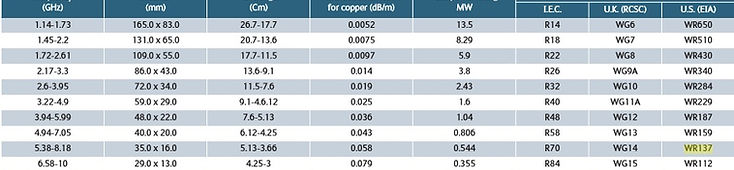
Let's assign lambda0 k0 lambdag beta Z0_TE Z0_TM to WR137 values
Following, beta Z0_TE and Z0_TM frequency dependencies
lambda0=c0/f0
m=1;n=0; % TEmn m=1 n=0
k0=2*pi*f0*(mu0*eps0*mur*er)^.5 % rectangular waveguide k0_TE=k0_TM
kc=((m*pi/a)^2+(n*pi/b)^2).^.5 % wave number for mode [m n]
fc=c0/(2*pi*er^.5)*((m*pi/a)^2+(n*pi/b)^2).^.5 % cut-off frequency
beta=(er*k0.^2-kc^2).^.5 % propagation constant when alpha=0
labmdac=2*pi./kc % cut-off wavelength
lambdag=2*pi./beta % group propagation wavelength
vp=2*pi*f0./beta % wave propagation velocity
alphad=k0^2*tand(d_skin)./(2*beta) % attenuation caused by metal
Z0_TE=k0*etha0/beta
Z0_TM=k0*beta/k0